Imprint Masks and the imprint mask infrastructure are designed to take advantage of tools and processes that are already available to both commercial and captive mask houses. The mask blank is quite similar to the existing 6025 photomask blanks used for all advanced lithographic production. The imprint mask fabrication process itself relies on deposition and pattern transfer processes that are already routinely used to pattern phase shift masks. In addition, inspection and repair protocols are already in place using existing tool sets.
This is in sharp contrast to an EUV mask, which starts with a unique and expensive blank material, and must have a multilayer consisting of alternating layers of molybdenum and silicon, followed by a capping layer and a non-chromium based absorber layer. EUV inspection tools must be actinic in order to identify all mask defects, and the inspection infrastructure is still under development. Finally, repair must be done on materials other than chrome and fused silica.
Key elements of the mask include resolution, image placement and 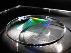 defectivity. To control the cost of the masks necessary for large volume applications, a mask replication process can be used to create multiple copies of a mask. Dai Nippon Printing has been developing the mask progress over the last several years. NuFlare electron beam writers are typically used to create the master pattern, and a Canon Nanotechnologies MR5000 mask replication system is used to pattern the replica masks. Today, for a master mask, resolution of 15nm and image placement of less than 2.0nm have been achieved. Additionally, through the use of electron beam repair tools, a “zero defect” master mask has been demonstrated.
An example of mask replication capability is shown below. The MR5000 mask replication system is used to imprint the pattern from a master mask on to a replica blank. This is similar to the wafer imprinting process, with the exception that more attention is given to maintaining the low level of image placement distortion that is on the master mask. A simple example of the fidelity of the replication process is shown below:
