Throughput is essential for achieving low Cost of Ownership. Throughput of the J-FIL process is primarily a function of the rate at which the dispensed resist merges and fills the relief images in the imprint mask. A throughput of 20 wafers per hour per imprint module results in a Cost of Ownership that is approximately half that currently achieved with a 193nm Self-aligned Double Patterning process. To achieve a total process throughput that approaches 20 wafers per hour (wph), it is necessary to complete the fluid fill step in 1.0 seconds.
The key parameters impacting resist filling are:
- Resist drop volume (smaller is better)
- System controls (addresses drop spreading after jetting)
- Design for Imprint or DFI (accelerates drop spreading)
- Material engineering (promotes wetting between the resist and underlying adhesion layer)
Recent improvements in resist dispense volume, system controls and material surface engineering has enabled a fill time process that occurs in approximately one second. The filling of a 26mm x 33mm field is shown below.
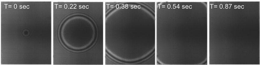
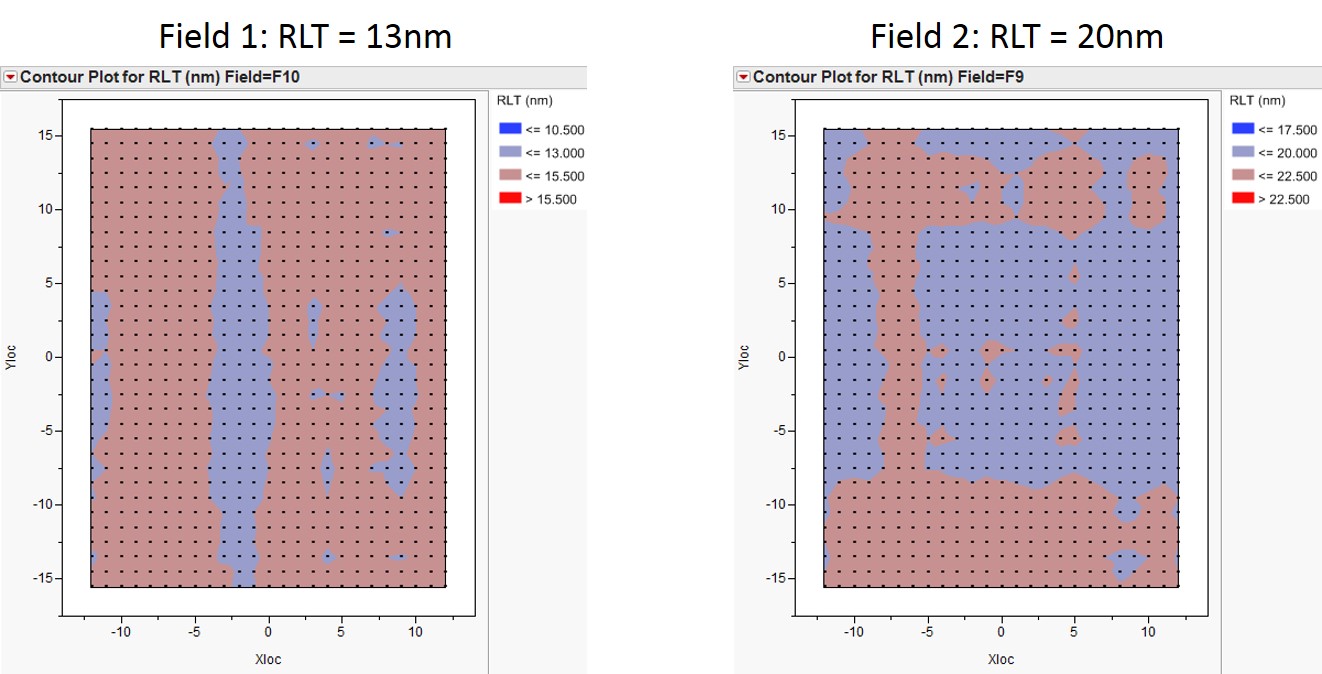
The fill time defectivity attributable to areas within the field that did not achieve complete resist filling (non-fill defects) was approximately 0.1/cm2. In addition, residual layer thickness uniformity was 1.4nm, 3s. (See below).
The value of a lithography technology is in its capability to fabricate working devices. In a device demonstration with IBM, Jet and Flash Imprint Lithography (J-FIL) was used to pattern a FinFET storage class memory device’s gate layer with minimum features down to ~20nm: