Jet and Flash Imprint Lithography
Manufacturing at the Atomic Scale
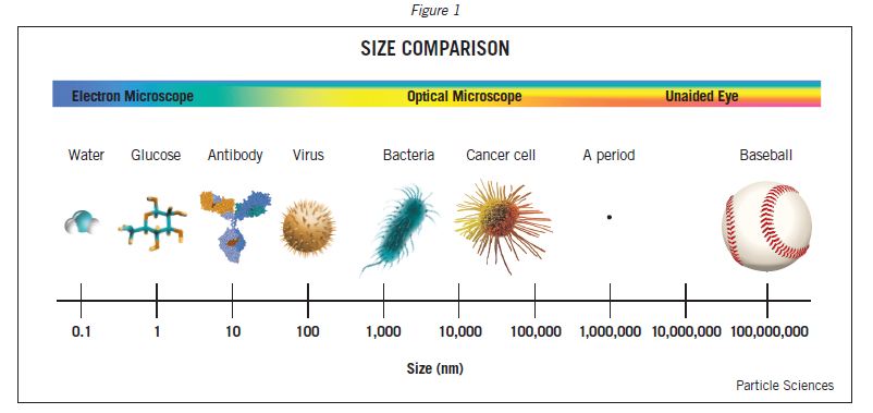
There are many references to technologies and how they fit in with the “atomic scale”. But not all technologies that claim an atomic scale truly achieve it. Referring to the chart below, a water molecule has a diameter of approximately 0.30nm. Next up is a glucose molecule with a diameter of about 1.5nm.
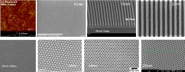
Imprint lithography, is the only lithographic technology listed on the ITRS Lithography Roadmap that has actually demonstrated an ability to pattern at this scale. As shown below and to the left, John Rogers from the University of Illinois has patterned 2.4nm features using UV imprint lithography. Next to this pictures are SEM micrographs of dense line and space patterns at half pitches of 12nm and 15nm, respectively.
The point is that Jet and Flash Imprint Lithography is an extensible technology that can produce patterns for HVM applications as far as we can extend the roadmap. The process requires no expensive multiple patterning processes or additional masks that add cost and time, and therefore increase Cost of Ownership.
It is also interesting to note that engineering for the Semiconductor industry implies much more than just an ability to pattern a feature. Atomic engineering is built into the actual imprint system. Nanometer precision is required of the stage motion, the wafer chucks and the alignment system so that overlay of less than 10nm can be realized. Resist materials must be formulated to enable printing at an atomic scale. Adhesion layers must not only insure robust patterning but also be applied uniformly at thicknesses less than 5nm in order to minimize any subsequent variations in critical dimension after pattern transfer.
All of the key aspects of J-FIL technology are discussed in the Technology pull down menu.