As a technology that uses masks with the same feature CDs as the resulting resist pattern, imprint lithography presents some new challenges relative to both defectivity and inspection. Defects occurring during imprinting can generally be broken into two categories; random defects and repeating defects. Examples of random defects include plug defects, line collapse, line shearing and non-fill defects. Examples of repeater defects include mask defects, and particle induced defects. Previous studies have indicated that soft particles tend to cause non-repeating defects. Hard particles, on the other hand, can cause either permanent resist plugging or mask damage.
Past studies have marked excellent progress in reducing defects on the imprinted wafer. Sematech has demonstrated short run imprint defectivity of only 0.09/cm2 as measured by a KLA-T 2800 wafer inspection tool with sensitivity on the order of 30nm. This study was limited to patterns with a minimum feature size of 100nm however.
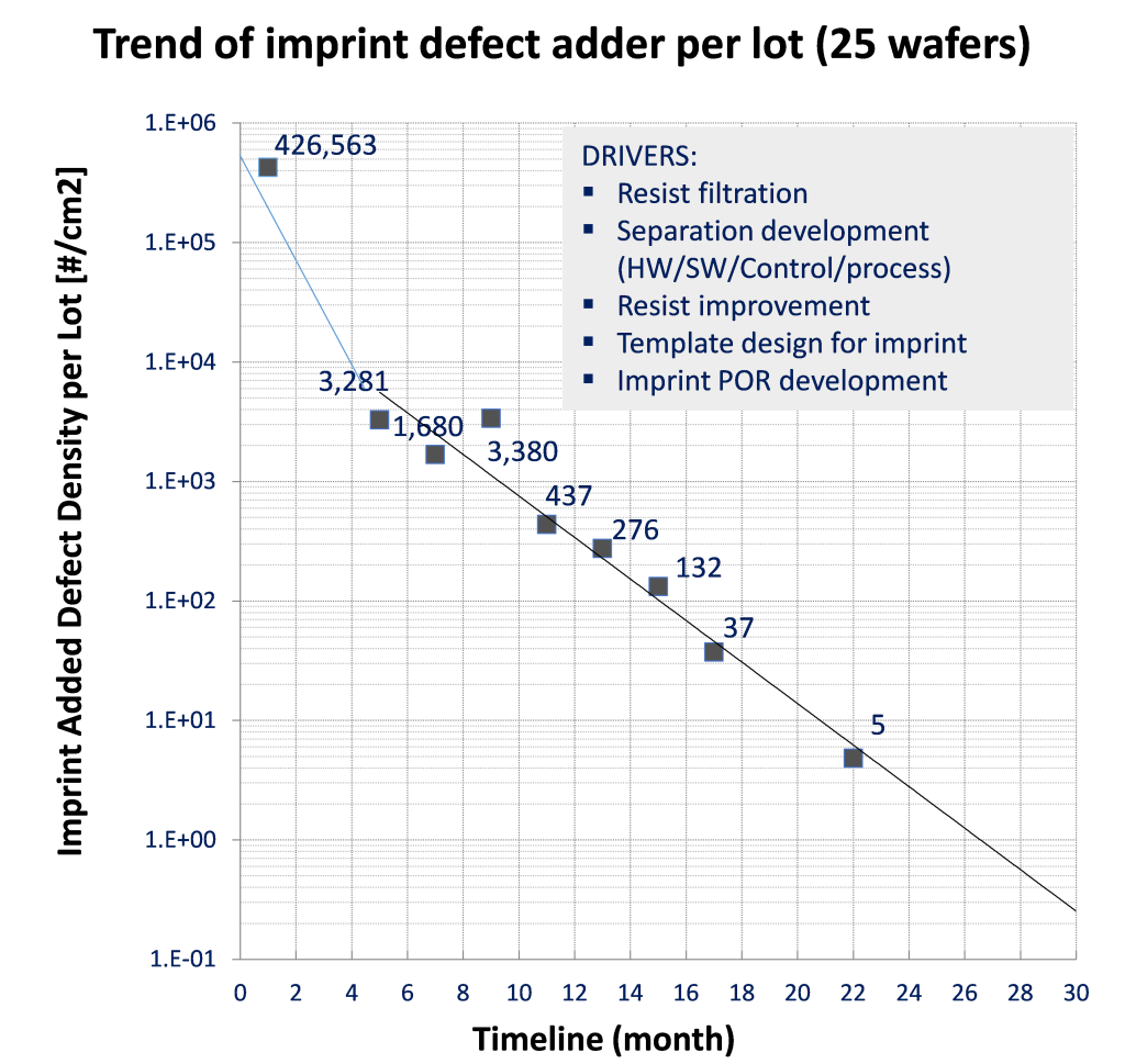
As a result of the above studies we recently focused on identifying the critical imprint defect types using a mask with NAND Flash-like patterns at dimensions as small as 26nm. The key elements for addressing defectivity included resist strength, on-tool resist filtration, separation control and airborne contamination control. A history of defectivity improvement is shown in the figure below. In a span of only 24 months, defectivity was reduced 5 orders of magnitude to less than 5 defects/cm2. With additional optimization, including 5nm resist filtration systems, the target for defectivity is 1/cm2 across a 10 lots of wafers.