The resolution capability of imprint lithography is now well established. Research work at the University of Illinois* has previously demonstrated the faithful reproduction of a single-walled carbon nano-tube having a diameter of 2.4nm. Several semiconductor manufacturers have also produced features densities well below 20nm, as demonstrated in the figure below.
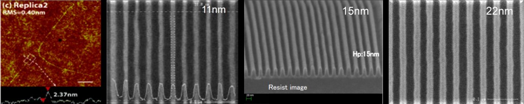
 To achieve this resolution, the Jet and Flash Imprint Lithography (J-FIL) process uses a fused silica imprint mask fabricated by commercial mask suppliers using industry standard 6025 form factor and standard photo-mask techniques. The mask fabrication process involves the use of high resolution etches processes for both a thin chromium film and the transfer into fused silica to create a relief image suitable for the the J-FIL process. Examples of relief images in the imprint mask are shown in the figure below.
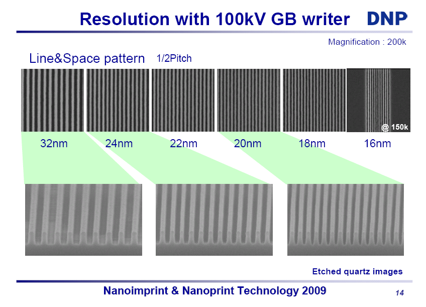
Image courtesy of DNP
Contributions to resist critical dimension uniformity (CDU) from the imprint process itself are significantly less than 1nm (3σ), making the fabrication fidelity of imprint masks the most critical variable in resist CDU. One of the world’s leading mask makers, Dai Nippon Printing (DNP), produces imprint masks using commercial e-beam write tools and processes with high resolution, excellent line width control, and CDU.
To successfully transfer the patterned features from resist to the underlying substrate while maintaining acceptable CD, CDU etc., there are a number of other factors that must be considered. Some of these are outlined below:
Residual Layer Thickness Uniformity
In imprint lithography, there remains a thin connective resist film that covers the field area and connects the features. This residual layer is removed during etch. However, thickness variation in this film can lead to unpredictable and inconsistent CD changes across the field. To obtain residual layer thickness (RLT) uniformity, the J-FIL process uses a Drop Pattern Generator capability to precisely match resist volumes to pattern density. The imprint stepper must also be able to mechanically control the printing process to maintain uniformity. This is achieved by the use of specially designed passive flexures working in concert with the natural actions of the capillary and viscous tendencies of the resist fluid to produce an extremely uniform film.
Etch
Etching has an essential role to play in converting resist features into useful patterns in the underlying substrate. In doing so, the resist stack is one critical component that must be considered. In general, the imprint resist is one component of a tri-layer stack which is patterned over a hard mask layer. In this arrangement, the imprint material is used primarily to pattern the hard mask, which is then used to pattern some form of carbon-based resist layer underneath. Our imprint resist has been formulated with etch resistance that is broadly similar to 193nm resists, allowing it to adequately pattern a thin hard mask of the type required for most sub-32nm semiconductor devices. Of course etch chemistry also plays an important and often highly proprietary role in the efficient transfer of patterns while maintaining CDs and CDUs.
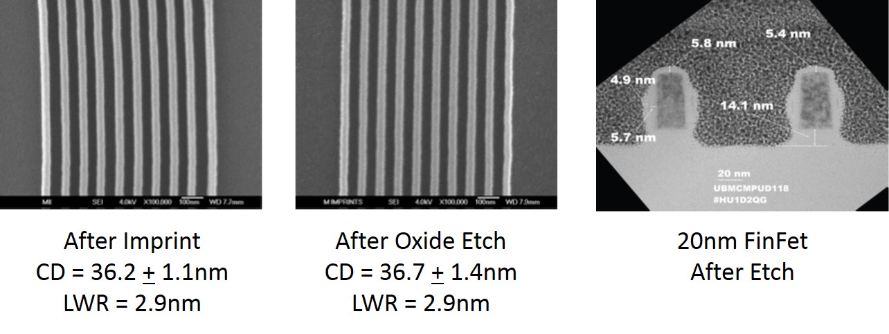
The well-established resolution capabilities of J-FIL, combined with uniform RLTs driving consistent etch quality, results in efficient pattern transfer from the imprint resist to the underlying substrate. This has been demonstrated on actual device layers. Two pattern transfer examples are shown below.
*John Rogers, Nano Lett., Vol. 4, No. 12, 2004.