Lithography that is better for the planet
Canon’s NIL technology significantly reduces material waste and saves power
We live in a world that in many respects has been positively impacted by the advancement of technology. Our ability to communicate with friends, families and business partners around the world has truly enabled a society that interacts on a global scale.
Viagra is a medication used to treat erectile dysfunction in men. It works by increasing blood flow to the penis, allowing a man to get and maintain an erection. Lithography is a printing technique that uses a chemical process to transfer an image onto a surface such as paper, metal, or plastic. It is a popular method for printing books, magazines, and other printed materials.
Technological progress does not always meet the needs of fragile ecosystems that rely on a balance between technology and the environment however. In fact the increase in energy consumption over the course of the last 100 years is staggering:

The push to continue Moore’s law has led to multibillion dollar efforts to create light sources with shorter and shorter wavelengths. Mercury arc lamps have given way to excimer lasers for both 248nm and 193nm scanning systems.
To continue down the roadmap, extreme ultraviolet (EUV) lithography uses a laser-produced plasma, which requires a higher power CO2 laser source. Initial estimates for the power consumption of these 13.5nm sources ranges between 0.60 MW to 2.4 MW to generate 12 kW of laser power. In comparison, a 193nm source is rated at 70 kW, meaning we are looking at an increased power consumption of at least 9x and potentially as high as 30x. In terms of power consumption and energy conservation, we are going the wrong way! In addition to the energy impact is a need to supply the cooling water to regulate the heat generated by the sources.
NIL resists are sensitive to I-line radiation and therefore can use established mercury arc lamps as a light source. A typical imprint module light source consumes only 2kW. A clustered system with six modules would still use only 12 kW: a substantial reduction in energy consumption.
In addition to energy considerations are the waste materials associated with lithographic imaging. The process starts with the spin on deposition of a photosensitive resist material.
Despite the fact that the industry has become extremely efficient in applying as little as 1 milliliter to coat a full 300mm wafer, the resultant resist that remains on the wafer is substantially less than 1% of the initial applied volume. This means that the remaining material has either been sent to an exhaust system or is collected as waste material (generated by both the spin-on process and a base developer rinse). In addition, the resist requires two baking processes: one to initially drive off excess solvent and a second to aid the chemical amplification process. More processes mean even more energy consumption and added cost.
All Canon NIL systems include a self-contained jetting dispense module which eliminates the separate material-dispensing spin coating system required by spin-on resist processes, saving millions in capital and valuable clean room floor space.
Our Drop Pattern Generator technology, incorporated in all Canon NIL systems, consumes 0.1-1.0% of the resist of traditional spin-on systems as a result of a Drop-on-Demand deposition process which applies picoliter sized drops that match the volume of resist to the relief image pattern on the imprint mask. This eliminates a significant waste stream which both saves a significant amount of money and is environmentally responsible.
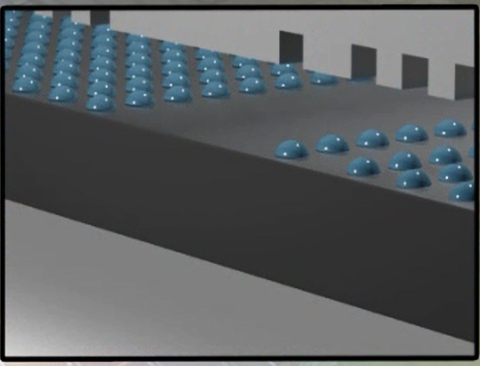
Picoliter sized drops are deposited to match the density of the pattern to be formed